Quilter
Quilter is a physics-based AI platform that automates PCB layout, transforming the design process from weeks to hours. …
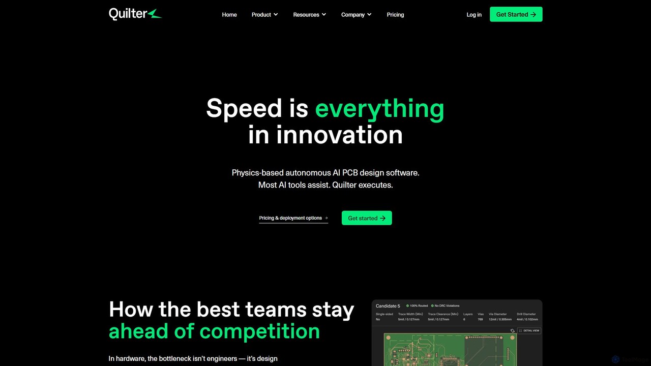
Quilter is a physics-based AI platform that automates PCB layout, transforming the design process from weeks to hours. It enables hardware teams to rapidly iterate on prototypes and test boards by autonomously handling component placement and routing. It integrates seamlessly with existing workflows and prioritizes IP security with options for on-prem deployment.
About Electronics Design Automation
Electronics Design Automation (EDA) tools are specialized AI-powered software solutions that streamline and optimize the entire electronic product development lifecycle. These tools leverage advanced algorithms, including machine learning, to automate complex tasks from circuit design and simulation to PCB layout and verification. They significantly accelerate the design process, reduce errors, and enable the creation of highly sophisticated and reliable electronic systems, forming a critical component within the broader field of engineering.
Core Features
- Circuit Design & Capture: Tools for schematic entry, component selection, and hierarchical design.
- Simulation & Analysis: Advanced simulators for analog, digital, mixed-signal, and electromagnetic analysis to predict circuit behavior.
- PCB Layout & Routing: Automated and interactive tools for physical placement of components and routing of interconnections on printed circuit boards.
- Verification & Testing: Methodologies and tools for functional verification, design rule checking (DRC), layout versus schematic (LVS), and test pattern generation.
- Logic Synthesis & Optimization: For digital designs, converting high-level descriptions (RTL) into gate-level netlists and optimizing for performance, power, and area.
Applicable Scenarios
EDA tools are indispensable for hardware engineers, semiconductor designers, and embedded systems developers across various industries. They are used in designing microprocessors, memory chips, communication systems, consumer electronics, and automotive control units, enabling rapid prototyping and rigorous validation of complex electronic systems before manufacturing.
How to Choose
Selecting an EDA solution requires evaluating its compatibility with specific design flows (e.g., analog, digital, RF), the breadth of its feature set for simulation and verification, integration capabilities with existing CAD/PLM systems, and the vendor's support and ecosystem. Consider also the scalability for future projects and the total cost of ownership, including licensing and training.
Electronics Design AutomationUse Cases
Automated PCB Layout Optimization
Hardware engineers designing complex multi-layer printed circuit boards (PCBs) utilize AI-powered EDA tools to automate component placement and trace routing. By inputting design constraints and performance targets, the tools generate optimized layouts that minimize signal integrity issues, reduce board size, and improve manufacturability, significantly cutting down manual design time and iteration cycles.
AI-driven IC Verification Acceleration
Semiconductor design teams employ advanced EDA verification tools integrated with machine learning to accelerate the functional verification of integrated circuits (ICs). These tools can identify potential design flaws, predict corner cases, and generate intelligent test benches more efficiently than traditional methods, drastically reducing the time and computational resources required to ensure design correctness.
Generative Design for Analog Circuits
Analog IC designers leverage generative EDA tools to explore novel circuit topologies and optimize performance parameters. By defining high-level specifications, the AI algorithms can automatically synthesize and evaluate numerous circuit configurations, providing innovative solutions for amplifiers, filters, and data converters that might be difficult to conceive through manual design, pushing the boundaries of analog performance.
FPGA Design and Synthesis Optimization
Embedded systems developers working with Field-Programmable Gate Arrays (FPGAs) use EDA tools to optimize logic synthesis, placement, and routing. AI algorithms within these tools can analyze design constraints and target device architectures to achieve better timing closure, reduce power consumption, and maximize resource utilization, leading to more efficient and higher-performing FPGA implementations.
Power Integrity Analysis with Machine Learning
Power electronics engineers and system architects apply machine learning-enhanced EDA tools for sophisticated power integrity (PI) analysis of complex electronic systems. These tools can predict voltage drops, current densities, and electromagnetic interference (EMI) issues across power delivery networks, helping designers proactively mitigate potential problems and ensure stable and reliable system operation.
Automated Test Pattern Generation (ATPG)
Test engineers in semiconductor manufacturing rely on EDA tools for Automated Test Pattern Generation (ATPG) to create efficient test vectors for detecting manufacturing defects in integrated circuits. AI algorithms can optimize these test patterns to achieve high fault coverage with minimal test time, ensuring the quality and reliability of mass-produced chips while reducing testing costs.