ToolMage
Sign in

Best 2 Electronics Design AI tools for Engineering

Popular Electronics Design AI tools in Engineering include Flux and SnapMagic, helping you work more efficiently.

Freemium

SnapMagic

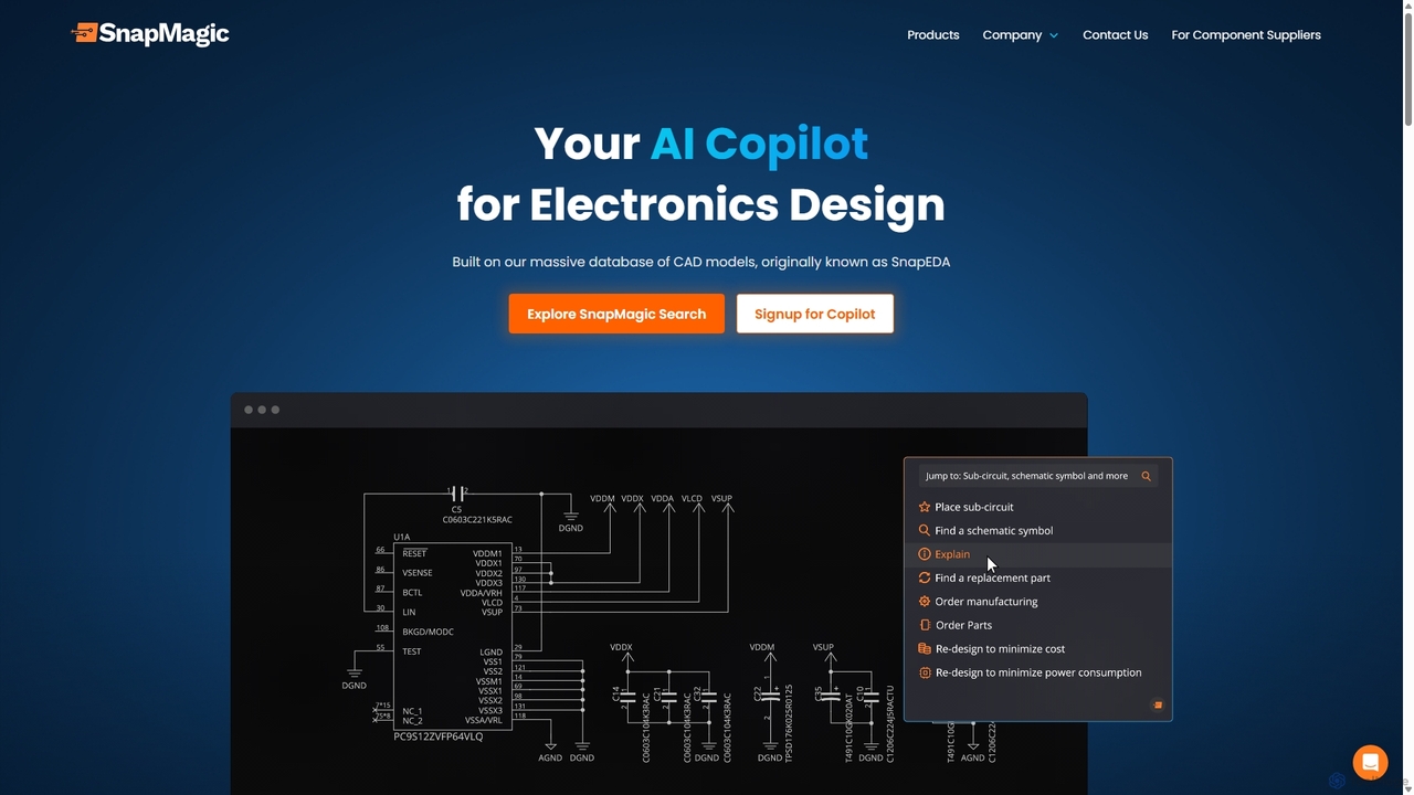
SnapMagic is an AI copilot for electronics design, automating and accelerating the circuit board creation process. It uses AI to auto-complete circuits, optimize your Bill of Materials (BOM) for cost and power, and provides real-time supply chain data. Engineers can interact with designs using natural language, streamlining repetitive tasks and fostering innovation from concept to manufacturing.

Hardware
Visits 59.5KFavorites 120Likes 128
Freemium

Flux

Flux is a modern, browser-based electronics design tool that leverages AI to revolutionize PCB creation. Its AI Copilot automates the tedious routing process with a single click, producing human-like, professional layouts. Designed for collaboration, Flux integrates a circuit simulator and a vast component library, making it accessible for beginners while offering powerful features for advanced engineers.

Hardware
Visits 699.1KFavorites 148Likes 151

About Electronics Design

AI Electronics Design tools are a specialized category of software that leverages artificial intelligence to automate and optimize the creation of electronic circuits, PCBs, and integrated circuits. These tools employ machine learning algorithms to analyze complex design constraints, predict circuit performance, and generate optimal layouts. They significantly accelerate the design cycle, reduce human error, and enable the development of more complex and efficient electronic systems. Unlike traditional EDA software, they offer predictive insights and generative capabilities for tackling advanced engineering challenges.

Core Features

  • Intelligent Schematic Capture: Automatically suggests components, completes connections, and performs real-time error checking based on design context.
  • Automated PCB Routing: Generates optimized routing paths for traces, considering signal integrity, thermal constraints, and manufacturing rules.
  • Predictive Circuit Simulation: Uses AI models to rapidly simulate circuit behavior and performance, identifying potential issues before prototyping.
  • Generative Design Optimization: Creates novel component placements and circuit topologies to meet specific performance targets like power efficiency or size reduction.

Use Cases

These tools are essential for hardware engineers, PCB designers, and semiconductor companies. They are applied in developing complex products like IoT devices, high-frequency communication systems, automotive electronics, and advanced microprocessors, where performance and time-to-market are critical.

How to Choose

When selecting a tool, consider the complexity of your designs (e.g., high-speed, multi-layer PCBs), integration with your existing toolchain (like CAD and simulation software), the specific AI features offered (e.g., routing vs. simulation), and the learning curve for your team.

Featured tool rankings

Electronics Design use cases

1

Rapid Prototyping of IoT Device PCBs

An engineer at a startup is tasked with designing a compact PCB for a new smart home sensor. Using an AI electronics design tool, they input the schematic and physical constraints. The AI autorouter then generates a fully routed, two-layer board layout in minutes, a process that would typically take hours of manual work. The tool optimizes for minimal size and ensures signal integrity for the wireless module, allowing the team to order a prototype board the same day and significantly accelerate their development timeline.

2

Optimizing High-Frequency Circuit Layouts

An RF engineer is designing a complex circuit for a 5G communication device. Signal integrity and impedance control are critical. They use an AI-powered tool to simulate electromagnetic fields and suggest optimal trace geometries and component placements. The AI analyzes thousands of potential layouts to minimize signal reflection and crosstalk, providing a design that meets strict performance specifications much faster than through manual iteration and traditional simulation methods.

3

Automated Verification of Complex ICs

A semiconductor design team is working on a new microprocessor with billions of transistors. Manually writing test cases to verify all functionalities is nearly impossible. They deploy an AI tool that analyzes the chip's design (RTL code) and intelligently generates test stimuli to target hard-to-reach corner cases and potential bugs. This AI-driven verification process identifies critical flaws earlier and achieves higher functional coverage, reducing the risk of costly chip respins after manufacturing.

4

Generative Design of Power Supply Schematics

An electronics hobbyist wants to build a custom power supply for a project but lacks deep design expertise. They use a generative AI tool, inputting key parameters like input voltage range, required output voltage, and maximum current. The AI then generates a complete and validated schematic for a buck-boost converter, including a bill of materials (BOM) with suggested components. This empowers users with less experience to create reliable and efficient circuits that are tailored to their specific needs.

5

Thermal Analysis and Management for PCBs

A designer creating a PCB for a high-power LED driver needs to prevent overheating. They use an AI design tool with integrated thermal simulation. The AI analyzes the component layout and power distribution, creating a detailed heat map of the board. It then suggests modifications, such as repositioning critical components, adding thermal vias, or enlarging copper pours, to improve heat dissipation. This predictive analysis helps avoid thermal failures in the final product without requiring multiple physical prototypes.

6

Component Selection and BOM Optimization

A hardware team is designing a cost-sensitive consumer product. The engineer defines the functional requirements for a specific circuit block. An AI tool then searches through vast supplier databases to recommend a list of compatible components. It optimizes the selection based on multiple criteria simultaneously: cost, stock availability, lead time, and performance specifications. This automates a tedious research process, reduces the total Bill of Materials (BOM) cost, and mitigates supply chain risks by suggesting alternative parts.

Electronics Design FAQ

What are AI Electronics Design tools?

AI Electronics Design tools are advanced software applications that use artificial intelligence and machine learning to assist in and automate the design of electronic systems. They go beyond traditional Electronic Design Automation (EDA) by not just following rules, but by learning from data to predict outcomes, optimize complex layouts, and even generate novel circuit designs. Key features often include intelligent schematic creation, automated PCB routing, and predictive performance simulation.

How do AI tools differ from traditional EDA software?

The primary difference lies in their core methodology. Traditional EDA (Electronic Design Automation) tools are largely rule-based and algorithmic; they execute specific commands given by an engineer. AI electronics design tools are learning-based and predictive. They can:

  • Optimize Holistically: AI can consider thousands of variables (thermal, signal integrity, cost) simultaneously for a globally optimized solution, whereas traditional tools often optimize one factor at a time.
  • Generate Novel Solutions: AI can propose new layouts or circuit topologies that an engineer might not have considered.
  • Accelerate Simulation: They use learned models to predict performance much faster than brute-force physics-based simulations.
In essence, traditional EDA is a powerful calculator, while AI EDA acts more like an experienced engineering assistant.

How to choose the right AI Electronics Design tool?

Selecting the right tool depends on your specific needs. Consider these factors:

  • Design Complexity: Are you working on simple two-layer boards or complex, high-speed, multi-layer designs? Ensure the tool's capabilities match your requirements.
  • Integration: How well does it integrate with your existing workflow, such as schematic capture software, CAD tools, and manufacturing outputs (Gerber files)?
  • AI Feature Set: Does the tool focus on AI-powered routing, simulation, component selection, or generative design? Choose one that solves your biggest bottleneck.
  • Learning Curve: Evaluate the user interface and available support. A powerful tool is only useful if your team can adopt it efficiently.
It's often beneficial to start with a trial version to assess its suitability for a sample project.

Who can benefit from using AI in electronics design?

A wide range of users can benefit from AI in electronics design, from individuals to large corporations. This includes:

  • Hardware Startups: To accelerate prototyping and reduce development costs, allowing them to compete with larger companies.
  • Experienced Engineers: To tackle highly complex designs (like high-density interconnects or RF circuits) and automate tedious tasks, freeing them up for more creative problem-solving.
  • Electronics Hobbyists and Students: To lower the barrier to entry for creating functional and reliable circuits without needing years of specialized experience.
  • Large Semiconductor Companies: To optimize chip floorplanning, automate verification, and improve manufacturing yield for next-generation processors.

What are the main advantages of using AI for PCB layout?

Using AI specifically for PCB layout offers several key advantages over manual or traditional autorouting methods. The main benefits include:

  • Superior Optimization: AI can analyze trade-offs between trace length, signal integrity, thermal performance, and manufacturability far more effectively than humans, leading to a more robust final design.
  • Significant Time Savings: AI can route complex, dense boards in minutes or hours, a task that could take a skilled designer days or weeks to complete manually.
  • Error Reduction: AI-driven routing adheres strictly to design rule constraints (DRC), minimizing the chance of human error that could lead to costly manufacturing defects.
  • Handling Complexity: It excels at routing high-speed interfaces (like DDR memory) and high-density interconnects (HDI) where manual routing is extremely challenging and error-prone.